What is Complex Programmable Logic Device?
What is CPLD(Complex Programmable Logic Device)?
The PAL (Programmable Array Logic) and GAL (Generic Array Logic) devices were combined to create the CPLD, also known as the Complex Programmable Logic Device, which is a sizable integrated circuit. Its size and complexity are both comparatively large. For this kind of digital integrated circuit, users can construct their own logic functions in accordance with their needs. The integrated development software platform generates the matching target file using schematic diagrams and hardware description language, which is then sent to the target chip via the download cable (referred to as "in-system" programming) to implement the specified digital system. An integrated circuit called a CPLD aids in the operation of digital systems. An FPGA, on the other hand, is an integrated circuit that is primarily made to be altered by a customer or a developer after production. Up to 100,000 tiny logic blocks can be found in FPGAs. FPGA can be used in Drone Innovation field and Radar System.
Evolution of CPLD
The subclass of the PLA known as Programmable Array Logic (PAL) is. It has a huge, programmable electronic component for ANDing inputs, just as the PLA. But the number of sentences that can be ORed together is constrained by the fixed nature of the OR plane. Latching devices, exclusive ORs, multiplexers, and other fundamental logic components enhance the inputs and outputs. It is crucial to incorporate timed components, frequently flip-flops.
The Complex Programmable Logic Device (CPLD), also known as the Complex Programmable Logic Device, is a substantial integrated circuit that was made by combining the PAL and GAL devices. The FPGA and SPLD, which are more complicated than the CPLD (complex programmable logic device), share functionality with the CPLD despite being simpler than it. CPLDs are less complex than FPGAs, but they are more complex than SPLDs. The PAL (programmable array logic), PLA (programmable logic array), and GAL (generic array logic) are the most often utilized SPLDs.
The Structure of CPLD
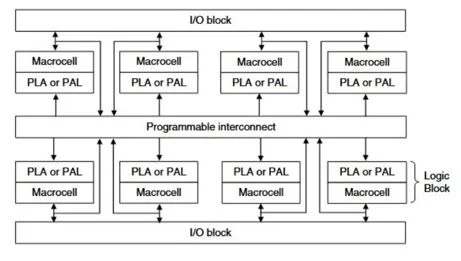
A CPLD is made up of three parts: an I/O block, a programmable interconnect channel, and a logic block.A programmable interconnect matrix cell (PIMC) at the center of the CPLD is encircled by programmable logic macro cells (MC, Macro Cell). The most complex of them all, the MC structure stands out as having a complex I/O cell interconnection structure that can be customized by the user to meet the needs of a particular circuit structure to carry out particular tasks. The timing of the suggested logic circuits may be reliably anticipated since each internal logic block in the CPLD is connected using fixed-length metal wires, avoiding the disadvantage of segmented connectivity topologies
A CPLD's logic blocks typically comprise 4 to 20 macrocells, each of which has a variety of product terms, product term assignments, and programmable registers, similar to a compact PLD. Each macrocell has a variety of configurations that can all be used in cascade to do more complex combinational and temporal logic operations. For highly integrated CPLDs, embedded array blocks with on-chip RAM or ROM are frequently provided. Programmable interconnect channels are used to provide a network connecting logic blocks, macrocells, and input and output pins. The interface between internal logic and a device's I/O pins is provided by I/O blocks. CPLDs with larger logic scales also typically have built-in JTAG boundary-scan test circuitry, which allows full and thorough system testing of programmed high-density programmable logic devices in addition to in-system programming via the JTAG interface.
CPLD Features
- Large density range and high performance.
- Non-volatile configuration memory and user-programmable ground pin functionality.
- Slew rate control for each output separately.
- Flexible 36 Vs 18 functional blocks.
- Flexible programming, high integration, short design and development cycle, wide applicability, advanced development tools, low design and manufacturing cost, low hardware experience for designers, no testing required for standard products, high confidentiality, and popular price are some of the features of CPLD.
- Electronic engineers now need to be proficient in the design and use of CPLD devices since they have grown to be an essential component of electronic goods.
- CPLD is frequently used in product prototyping and product manufacturing (typically below 10,000 pieces) because it can realize bigger scale circuit design.
CPLD programming
The programming languages for CPLDs are Verilog and VHDL, while the development tools are quartusII, ISE, etc. A logic design can be described using VHDL, a hardware description language (HDL). A configuration file that may be put into an FPGA or CPLD to implement the logic design is created when software tools scan a VHDL logic design. The name VHSIC Hardware Description Language is abbreviated as VHDL. A Very High-Speed Integrated Circuit is what this is. Here is an example of the design flow for the chip used in the snatcher's ornamentation. Most of the work done by the CPLD is done on computers. Here are the steps for programming a CPLD:
7128 The test is turned on once the chip has been pinned out and after the digital tube, snatch switch, indicator, and buzzer have been wired to the chipboard. The associated bit of the indicator should turn on when the snatch switch is depressed. Check to see if the results are added appropriately on the digital display after the judge adds points. If flaws are found, the hardware description language schematic diagram can be changed to correct the design.
Once the design is finished, new CPLD chips can be quickly copied for mass production; that is, the code can be written. To develop further designs for the chip, such as traffic light designs, you must once more write the hardware description language or sketch the schematic diagram. Then, to complete the design, repeat the previous stages. Similar to rebuilding a home, this design alteration is made possible by CPLDs, which allow for tens of thousands of iterations.
Pros and cons of CPLD
Pros of CPLD
- CPLD is simple to design.
- CPLD was developed at a modest cost.
- It aids in reducing the size of the board.
- High reliability is provided by CPLD.
- Ownership cost.
- More sales of the goods.
- The market is reached after fairly brief development cycles.
- Faster creates revenue more quickly.
Cons of CPLD
- CPLD is a more sophisticated programmable logic device than SPLD.
Xilinx CPLD vs. FPGA
|
|
FPGA |
CPLD |
|
Applicable design |
Complex timing functions |
Simple logic functions |
|
Interconnection Structure |
Distributed, rich cabling resources |
Aggregate, relatively limited cabling resources |
|
Confidentiality |
Generally less private. Although it is difficult to implement encryption on a general-purpose FPGA, some modern devices that use flash + SRAM technology (like Lattice's xp series, etc.) in the internal linkage of the loaded flash can offer a higher level of confidentiality. |
Generally better confidentiality |
|
Cost and price |
High price and cost |
Low price and cost |
|
Structural process |
The implementation method for the majority of the LUT plus register structure is primarily SRAM and also includes Flash, Anti-Fuse, and other operations. |
Product phrase; the predominant process is E2CMOS; additional processes include EEPROM, Flash, Anti-Fuse, and others. |
|
Number of flip flops |
Many |
Few |
|
Pin to pin Time Delay |
Unpredictable. For FPGAs, timing constraints and simulation are very important. |
Fixed |
|
Scale and Logical Complexity |
Large scale, high logic complexity, and new devices up to the trillion gate level. |
Small size and low logical complexity |
|
Programming and configuration |
There are typically two types: online programming using an MCU or DSP and external BootRom. Most of them are essentially RAM types, and when the power is turned off, the program is lost. In contrast to current FPGAs with inbuilt Flash or EECMOS, such as Lattice's XP device family, anti-fuse process FPGAs, like several of Actel's device families, typically retain their original logic configuration after a power failure. |
There are two ways to program a device: using a programmer to write ROM and using ISP mode, which is more practical because the software will not be lost when the device is powered off. |
Conclusion of CPLD vs. FPGA
FPGAs have distributed and rich cabling resources, while CPLDs have aggregate and relatively limited cabling resources. In FPGAs, the implementation method for the majority of the LUT plus register structure is primarily SRAM and also includes Flash, Anti-Fuse, and other operations, while in CPLDs, mostly product term, process is mostly E2CMOS, also contains EEPROM, Flash, Anti-Fuse and other different processes. The transition from discrete logic devices to entry-level FPGAs is made possible by simple programmable logic devices (SPLDs) and complex programmable logic devices (CPLDs), which are less complex components. Low power consumption, low logic density, and minimal complexity per chip are the main features of entry-level FPGAs. Devices with enhanced functionality add functional blocks with particular functions: A few examples include high-speed transceivers, Ethernet MACs, PCI express controllers, phase-locked loops (PLLs), high-speed serializers, and deserializers.
Application scenarios of CPLD
Once more, CPLD utilization speeds up and streamlines the product development process. Simulators can be run throughout development, allowing for the modification and customization of specifications as well as reducing development risk. Additionally, just like with many PLDs, designing without physically building the circuit is made simpler by the use of hardware description languages.
The rate at which new products are developed today is accelerating. There are numerous new things as you look around. It is safe to state that CPLDs are essential for such contemporary businesses' product development processes.
CPLD FAQ
What is the CPLD?
The PAL and GAL devices were combined to create the CPLD, also known as the Complex Programmable Logic Device, which is a sizable integrated circuit. Its size and complexity are both comparatively large. For this kind of digital integrated circuit, users can construct their own logic functions in accordance with their needs.
What does CPLD stand for?
Using CPLD technology, field programmable gate array configuration data are loaded from non-volatile memory. CPLDs are frequently used in a range of applications due to their tiny size and low power consumption, such as in price-sensitive, battery-operated portable devices.
Differences between CPLD and FPGA
Contrary to CPLDs, which have aggregate and comparatively meager cabling resources, FPGAs have widely distributed and rich cabling resources. In FPGAs, the majority of the LUT plus register structure is implemented using SRAM, along with other operations like Flash and Anti-Fuse. In CPLDs, the majority of the product term is implemented using E2CMOS, along with additional operations like EEPROM, Flash, and Anti-Fuse.
Why choose CPLD over FPGA?
Since CPLDs have bigger regions to implement more logic configurations, they are faster than FPGAs. A CPLD has two different types of interconnects: adjustable logic interconnect and programmable interconnect.


